This post is not a step-by-step tutorial. It's more of a "here's what I learned, here's why it's interesting, and here are the places I hit walls" kind of thing. If you're into LLMs, FPGAs, or just enjoy watching someone throw themselves at a hard problem, read on.
The Magic of BitNet: When Multiplication Becomes Addition
The whole story starts with BitNet, a framework from Microsoft Research. The core idea is deceptively simple: instead of storing the weights of a neural network as 16-bit or 32-bit floating point numbers, what if you only used three values — -1, 0, and +1? That's 1.58 bits per weight (log₂(3) ≈ 1.58), which is where the name BitNet b1.58 comes from.
"Okay, but surely the model gets dumb if you throw away all that precision?" — that was my first thought too. And yes, there's a quality tradeoff. But the BitNet b1.58-2B-4T model (2 billion parameters, trained on 4 trillion tokens) produces surprisingly coherent text. There's real potential here — good enough to have a useful conversation with.
Now here's where it gets interesting for hardware people.
In a normal neural network layer, computing an output requires a matrix-vector multiply: for each output neuron, you take a row of weights, multiply each weight by the corresponding input, and sum everything up. This is called a multiply-accumulate (MAC) operation. GPUs are fast at this because they have thousands of little MAC units running in parallel.
With ternary weights (-1, 0, +1), the multiply becomes trivial: - weight = 0 → result is 0, skip it entirely - weight = +1 → result is just the input value (multiply by 1 = do nothing) - weight = -1 → result is just the negated input value (subtract instead of add)
There is no floating point multiplication. The entire matrix-vector multiply collapses into: for each weight, either add the input, subtract the input, or do nothing. Pure addition and subtraction, controlled by 2-bit flags.
This is a massive deal for FPGAs. FPGAs are not fast at floating point multiplication — that burns a lot of DSP blocks and runs slowly. But FPGAs are extremely good at bitwise logic and fixed-point addition. An adder is just a chain of logic gates. You can pack thousands of them into a mid-range FPGA and run them at hundreds of megahertz.
BitNet essentially turns an LLM inference problem into a problem that FPGAs are naturally good at. That's the magic.
Why the KV260?
Once I decided to try this, I needed an FPGA board. The options range from hobbyist-level to serious datacenter cards (Alveo U250 — looks tempting). I landed on the AMD Kria KV260 Vision AI Starter Kit, and I'd make the same choice again.
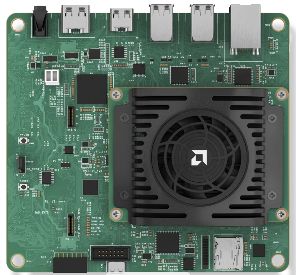
Here's why:
It's actually buyable. At the time of writing you can get one from a reputable distributor for a few hundred dollars.
The silicon is not trivial. The KV260 is built on the K26 SOM, which pairs a quad-core Cortex-A53 CPU with a Xilinx Zynq UltraScale+ FPGA fabric. The PL (Programmable Logic) side gives you:
- ~117K LUTs (logic cells)
- ~312 DSP blocks
- ~144 BRAM tiles (block RAM, 18KB each)
- 64 URAM tiles (UltraRAM, 288KB each — fast on-chip SRAM, this matters a lot)
- 4GB LPDDR4 shared between CPU and FPGA
That's enough to build something real.
The software ecosystem is decent. Xilinx/AMD provides Vitis HLS, which lets you write accelerator kernels in C++ and compile them to hardware. There's also the XRT (Xilinx Runtime) and tools like xmutil for loading and unloading overlays (partial bitstreams) without rebooting. The KV260 runs Ubuntu, so deployment feels relatively normal — copy some files, run a command, done.
You can prototype fast. The overlay system means I can synthesize a new hardware design on my desktop machine, SCP three files to the board, and be running it in minutes. No JTAG dance, no special programmer.
Most importantly, it runs Linux — I'm right at home.
The GEMV Kernel: Teaching an FPGA to Do Matrix-Vector Multiply
The hot loop in LLM decode (generating one token at a time) is GEMV — General Matrix-Vector multiply. For each transformer layer, the model multiplies a weight matrix (rows × columns) by an input vector. With BitNet, the weights are ternary.
For the BitNet b1.58-2B-4T model, the biggest GEMV calls have matrices of up to 6912 × 2560. That's 17.7 million weight elements, each being -1, 0, or +1. We need to do this roughly 210 times per token.
The Adder Tree
The core of my FPGA kernel is an adder tree. Here's the intuition:
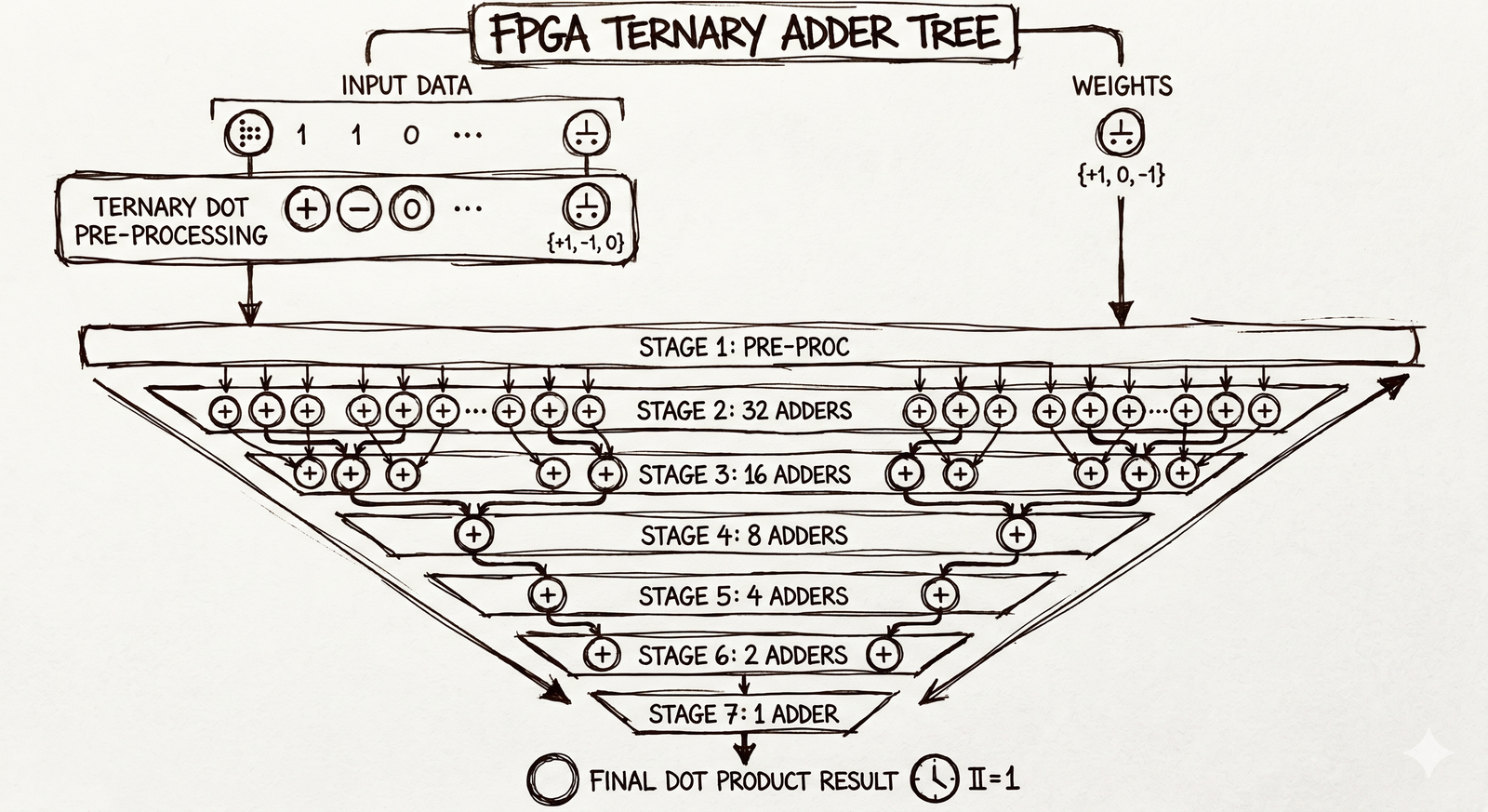
Imagine you have 64 input values and 64 corresponding ternary weights. You want to compute their dot product. In software, you'd loop over all 64 pairs and accumulate. On an FPGA, you can do something much more parallel:
- For each input value, look at its weight:
- if +1: pass the value through as-is
- if -1: negate the value (flip sign)
-
if 0: output zero
-
Now you have 64 signed values. Add them in a tree structure: first add pairs (32 additions happening simultaneously), then add those results in pairs (16 additions), and so on. Eight levels of additions, all happening in pipeline stages.
The entire dot product of 64 elements computes in ~8 clock cycles of pipeline latency, with a new result coming out every clock cycle (II=1, in HLS terminology). At 200MHz, that's one 64-wide dot product result every 5 nanoseconds.
In my implementation, I use 6 parallel ports to the weight memory (each port loading a different part of the weight matrix simultaneously), each handling 64 weights per clock. So every clock cycle, I'm processing 384 weight-input products in parallel. The accumulator then sums these across the K dimension to build up the output vector.
Why This Beats CPU So Decisively
On a Cortex-A53 (the CPU inside the KV260), even with NEON SIMD vectorization, you can do at most 16 int8 multiply-accumulates per cycle, at maybe 1.2GHz effective. For a 2560×2560 ternary GEMV, that's on the order of milliseconds just for the arithmetic.
The FPGA kernel, despite running at a more modest 200MHz, completes all 210 GEMV calls in ~73ms per token. On pure CPU, the equivalent workload would be closer to 500ms+.
The key insight is parallelism. The FPGA doesn't loop over the matrix — it spreads the computation across physical logic resources that all work simultaneously. This is exactly the kind of workload FPGAs were designed for.
Prior Art: The TeLLMe Paper
While I was deep in this project, I came across an arXiv paper that I wish I'd found earlier: TeLLMe v2 (arXiv: 2510.15926) — a team that implemented BitNet inference on the KV260 as a proper research project. They tackle the same problem on the same board, which makes the comparison direct.
Where our approaches diverge most is in how the FPGA actually computes the ternary dot products.
My approach is the adder tree described above: for each weight, conditionally negate or zero the activation, then reduce everything through a binary tree of adders. It maps naturally to Vitis HLS because it's just arithmetic expressed in C++.
TeLLMe takes a LUT-based approach. The key insight is that a 6-input Xilinx LUT can evaluate any boolean function of 6 bits in a single clock cycle. Since each ternary weight only needs 2 bits to represent, a single LUT can simultaneously encode the conditional negate/zero logic and compute a partial sum for three weight-input pairs at once. Instead of routing individual add/subtract operations through a chain of arithmetic primitives, the computation is folded directly into the FPGA's lookup table fabric — the lookup table is the computation.
The tradeoff: the LUT-based approach squeezes more operations out of each FPGA resource, but requires lower-level RTL implementation — or heavily annotated HLS — to prevent synthesis tools from inferring conventional adder logic instead. My adder tree is more straightforward to implement and reason about, but leaves some efficiency on the table compared to what the fabric can theoretically deliver.
Reading their paper after building my own thing was a strange experience — validating in some ways ("okay, I wasn't crazy for thinking this was tractable"), humbling in others ("they thought of several things I didn't"). If you want a more rigorous treatment, the TeLLMe paper is the place to go. My project is a solo weekend-turned-weeks exploration; their paper is a proper systems research contribution.
The Wall I Hit: DDR4 Memory Bandwidth
Here's where I have to be honest about the limitations.
My FPGA kernel can theoretically process weight data much faster than it actually does. The adder tree is hungry — it wants to consume hundreds of gigabytes of weight data per second to stay fully utilized. But the DDR4 interface on the KV260 tops out at around 19 GB/s of sustained read bandwidth.
For a single GEMV call (M=2560, K=2560 ternary weights, packed at 2 bits each): - Data to read: 2560 × 2560 × 2 bits = ~1.6 MB - At 19 GB/s theoretical bandwidth: could do it in ~85µs - My kernel time across all 210 GEMV calls: ~73ms per token, averaging ~350µs per call
The adder tree finishes its work long before the next chunk of weight data arrives from DDR. The FPGA fabric is waiting on memory, not the other way around. This is the classic memory-bound problem that plagues matrix operations on any hardware.
The weights (1.7 GB total for the 2B model) don't fit in the on-chip URAM (I only have ~2MB of it). So every GEMV call re-fetches the same weights from DDR. No matter how fast my adder tree is, I'm fundamentally limited by how quickly I can shovel data off the memory bus.
I keep imagining what it would look like if the weights could stream into the kernel continuously, with tokens flowing out at full compute rate. A device with HBM — offering hundreds of GB/s of bandwidth — might actually get there. That's an experiment I'd like to run someday.
A Glimpse at GEMM
There's a more natural fit for this kind of computation: GEMM (General Matrix-Matrix multiply), which is what happens during the prefill phase — when the model processes your input prompt all at once.
In GEMM, instead of multiplying a weight matrix by a single input vector, you multiply it by a whole batch of input vectors simultaneously. The weight data gets loaded from DDR once and reused across multiple computations. The arithmetic intensity (ratio of operations to memory transfers) goes way up, which is exactly what you need to hide the DDR bandwidth bottleneck.
In my latest implementation, I have a GEMM kernel that processes 8 tokens at a time (T=8 tile). Prefill throughput reached 23.26 tok/s for a 57-token prompt, compared to 4.41 tok/s for single-token decode — a ~5× improvement just from batching, because the weight data gets amortized across 8 tokens instead of 1.
But GEMM deserves its own article. The optimization story there — tiling, URAM buffering, double-buffering to overlap data load with computation — is a whole separate journey. I'll save it for part two.
Where Things Stand
Here's the full picture across iterations:
| Configuration | Prefill | Decode | Notes |
|---|---|---|---|
| Pure ARM CPU (4 threads, no FPGA) | 5.24 tok/s | 3.03 tok/s | Cortex-A53 NEON SIMD, Stage 0 baseline |
| FPGA: GEMV v3 + GEMM T=4 (Phase 2d) | 16.96 tok/s | 3.77 tok/s | First working GEMV+GEMM, 207-token prompt |
| FPGA: GEMV v6 + GEMM T=8 (Phase 4b, latest) | 23.26 tok/s | 4.41 tok/s | 6-port adder tree, T=8 tile, 57-token prompt |
The FPGA acceleration is real: prefill is 4.4× faster than pure CPU, and decode has improved meaningfully across iterations even as it remains memory-bound.
Is 4.41 tok/s fast enough to be practical? Honestly, not quite — it sits below the threshold where text feels responsive in real time. But it's running a 2-billion-parameter language model on a $250 board that fits in the palm of your hand, with no GPU and fully open hardware and software.
I find that pretty remarkable for where we started.
The main bottleneck — DDR bandwidth for decode — is a fundamental physical constraint, not something I can engineer around with cleverer HLS code. Addressing it properly requires either moving to a different memory architecture (HBM, anyone?) or amortizing the memory bandwidth cost across more computation, which brings us back to GEMM.
More on that next time.